4x4 INT Systolic Architecture Based Accelerator for Efficient Matrix Multiplication
Plan
The documentation is divided into two main sections:
- User’s Guide: Includes everything needed to use the chip.
- Developer’s Guide: Contains complete details of the chip, including internal signals, STGs, diagrams, etc. This section is made so that anyone who wants to integrate the chip into their own design can do so using this documentation.
User Guide
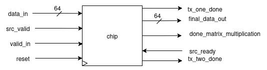
- The array takes an input of 64 bits and gives an output of 64 bits.
- This I/O is communicated using the bidirectional ready-valid protocol.
- The bits have a predefined format according to which they are received/transmitted.
Matrix Transfer Format [1st 2nd 3rd 4th ] [5th 6th 7th 8th ] [9th 10th 11th 12th] [13th 14th 15th 16th]
Input format:
- [63:32] → row (8 bits per element)[4 elements]
- [31:0] → column (8 bits per element)[4 elements]
Output format:
[2 × (32-bit elements)]
How to Give Input?
- Provide four chunks of 64-bit input where:
[63:32]contains the i-th row[31:0]contains the j-th column- In this way, each row/column will be 32 bits, and each element will be 8 bits (since
8 × 4 = 32). - These I/Os follow the ready-valid protocol:
- At the input end → valid is expected from the end user.
- At the output end → ready is expected from the end user.
Final Transfer
- Recognized with the
done_matrix_multiplicationflag being set. - This indicates:
- The availability of the final two elements from the array.
- The chip has returned to its idle state and is ready to accept new inputs.
Getting Started
Steps 1:
Clone the repository:
Clone our repository https://github.com/ee-uet/systolic-MAC.git by:
git clone git@github.com:ee-uet/systolic-MAC.git
Step 2:
Install All the Required Pre-requisites:
- Modelsim / Questasim
- GTK-Wave
- install
make - gcc --> for benchmark
Step 3:
Using Makefile :
You can see the simulations in GTK-Wave using the Makefile. You have to write following command :
make TOP=module_name all
Or you can alternatively use Modelsim or Questasim as well !
Developer’s Guide
Conceptual Overview
What is a Systolic Array?
- In parallel computer architectures, a systolic array is a homogeneous network of tightly coupled data processing units (DPUs) called cells or nodes.
- Each node or DPU:
- Independently computes a partial result as a function of the data received from its upstream neighbours.
- Stores the result within itself.
- Passes it downstream.
Applications of Systolic Arrays
🔹 Deep Learning Accelerators (ML)
Efficiently perform parallel matrix multiplications in neural networks like CNNs and Transformers.
🔹 Image & Signal Processing (DSP)
Enable real-time convolution operations for filtering, edge detection, and motion estimation.
🔹 DNA Sequence Alignment (Biology)
Accelerate alignment algorithms like Smith-Waterman using parallel dataflow for fast genome matching.
🔹 MIMO Signal Processing (DSP/Comms)
Support high-throughput matrix operations for channel equalization and beamforming in wireless systems.
...and much more.
Main Parts of a Systolic Array
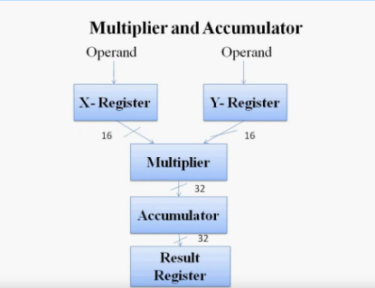
1. MAC Unit
- In computing, especially digital signal processing, the Multiply–Accumulate (MAC) or Multiply–Add (MAD) operation is a common step that:
- Computes the product of two numbers.
-
Adds that product to an accumulator.
-
The MAC operation modifies an accumulator
y:
y ← y + (a × b)
For simplicity, in C code:
y += (a * b);
- General CPUs are used in Von Neumann architecture, but digital signal processors (DSPs) use MACs.
- The hardware unit that performs the operation is known as a Multiplier–Accumulator (MAC Unit).
2. Processing Elements / Data Processing Units
- A Processing Element (PE), also called a Data Processing Unit (DPU), is the fundamental building block of a systolic array.
- Each PE is designed to perform simple operations such as:
- Addition
- Multiplication
- MAC (Multiply–Accumulate)
- PEs are connected to their neighbors in a regular pattern, allowing data to flow step by step.
- Together, many PEs work in parallel to achieve high throughput in matrix and vector computations.
3. Systolic Array
- A systolic array is a grid of interconnected Processing Elements (PEs) arranged in rows and columns.
- Data pulses rhythmically through the array like blood through the heart (hence the name “systolic”).
- The structure enables efficient parallel computation of linear algebra operations, especially:
- Matrix multiplication
- Convolution
DESIGN OVERVIEW
Specialty & Performance
- We built the entire Systolic Array completely from scratch, covering all modules and interconnections.
- On a 3 GHz machine, the full computation completed in just ~15 ns.
- This results in a performance that is nearly 50-160 times faster than a general purpose cpu(check the benchmarks section).
Explanation of Our Design
(1) MAC Unit
1. PinOut
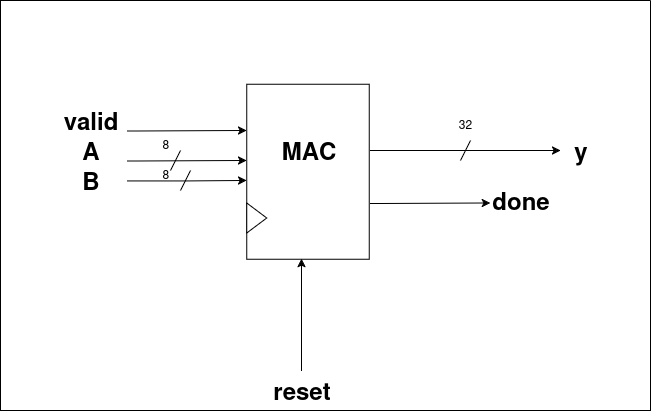
Inputs
- Takes the following as inputs:
- valid
- A (8-bit element of matrix)
- B (8-bit element of matrix)
- reset
Outputs
- Provides the following as outputs:
- y → 32-bit result
- done → 1-bit signal which goes high whenever
yis valid, indicating that the MAC unit has completed the operation.
2. Design Diagram
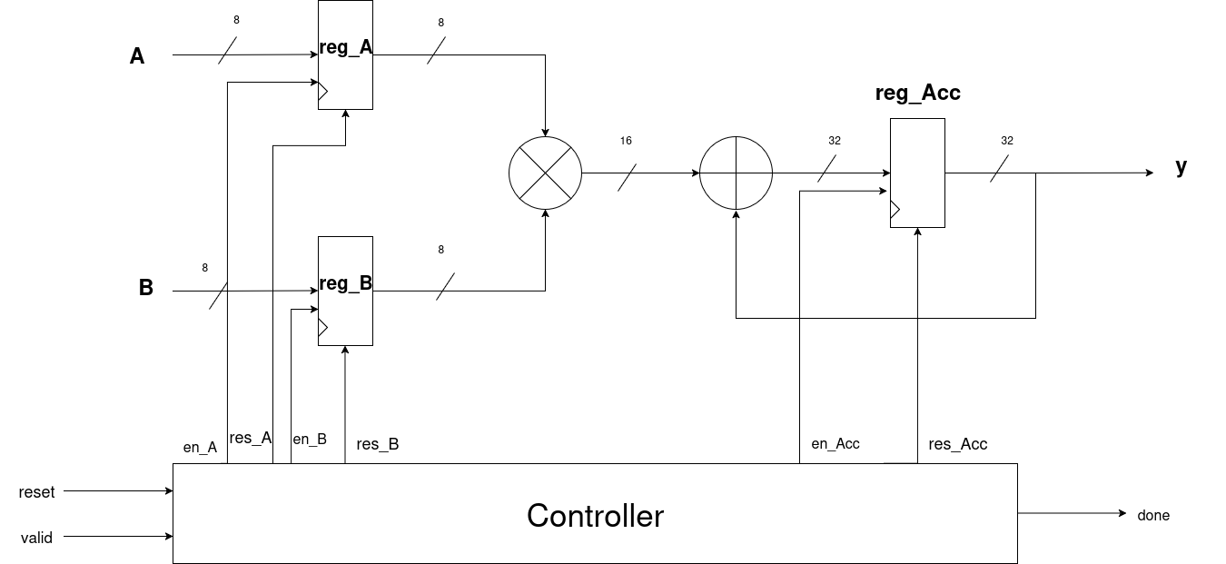
Explanation
- First of all, the user enters elements A and B.
- As soon as reset is off and valid becomes high:
en_Aanden_Bgo high.- The user-entered A and B values are stored in their respective registers:
reg_Aandreg_B. - Then:
- Both values are multiplied.
- The result is added to the previous result (principle of MAC).
- A register named reg_Acc stores the result whenever
en_Accgoes high. - (When
en_Accgoes high will be explained in the STG section.) - Since both input elements are 8 bits:
- Multiplication produces a 16-bit result.
- This result is padded to 32 bits → giving output
yas 32 bits. - As soon as the result
yis obtained, the done signal goes high.
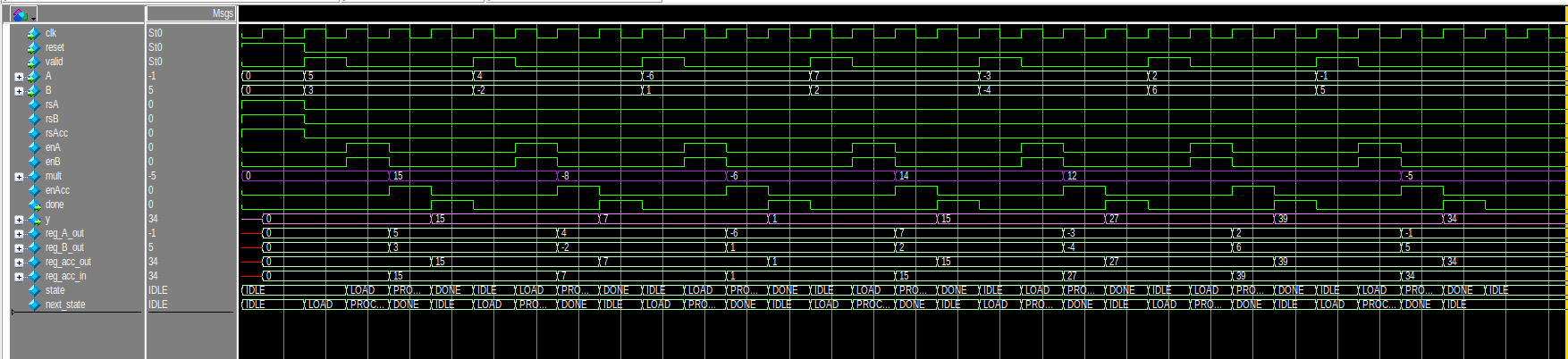
Simulations:
3. Register Design
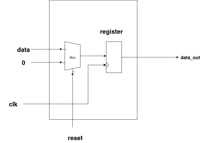
- This is the general register design used for all the registers in our system.
- First, a 2×1 MUX is used, whose output is stored into a register.
- The selector pin of the MUX is
reset. - Behavior:
- When reset = 0 (off) → The MUX selects input data, which is stored in the register. The corresponding
data_outis available in the next cycle. - When reset = 1 (high) → The MUX selects zero, and hence the register outputs
0asdata_out.
4. State Transition Graph (STG)
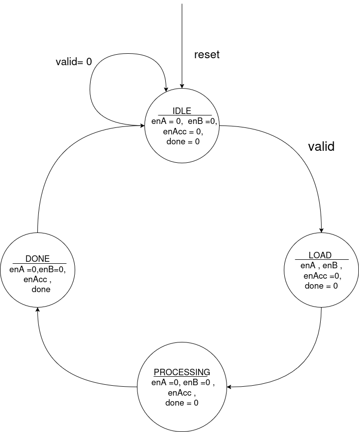
Explanation
I. IDLE
- Whenever reset = 1, the system enters the IDLE state:
- All register enables are low.
done = 0.- It remains in IDLE if
valid = 0. - When a valid signal is received, it transitions to the LOAD state.
II. LOAD
- In this state:
- Enables of reg_A and reg_B go high → user inputs are stored in
reg_Aandreg_B. - reg_Acc is still off (no computation yet).
done = 0since no result is available yet.- Next, it transitions to the PROCESSING state.
III. PROCESSING
- In this state:
- reg_A and reg_B enables go low (to hold current inputs and avoid taking new ones).
- reg_Acc enable goes high → computation starts, and result is stored in the accumulator.
done = 0since computation is still ongoing.- Next, it transitions to the DONE state.
IV. DONE
- In this state:
- en_A and en_B remain off.
- en_Acc stays on.
- The done signal = 1 → indicating completion of computation.
- Finally, it transitions back to IDLE, and the cycle continues.
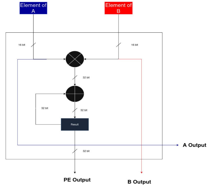
(2) PROCESSING ELEMENT (PE)
PinOut:
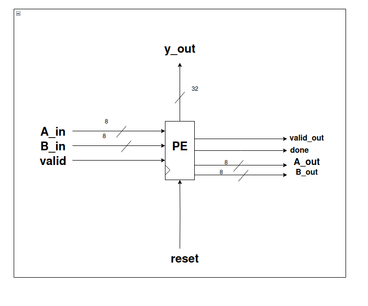
Inputs:
- valid, reset, A_in, B_in as inputs.
- A_in, B_in are 8-bit signals.
Outputs:
- A_out, B_out, done, valid_out, y_out.
- A_out, B_out are 8-bit signals.
- done goes high whenever the MAC operation completes.
- valid_out goes high whenever the overall PE operation completes.
- y_out is the 32-bit output of the PE.
2. Design Diagram
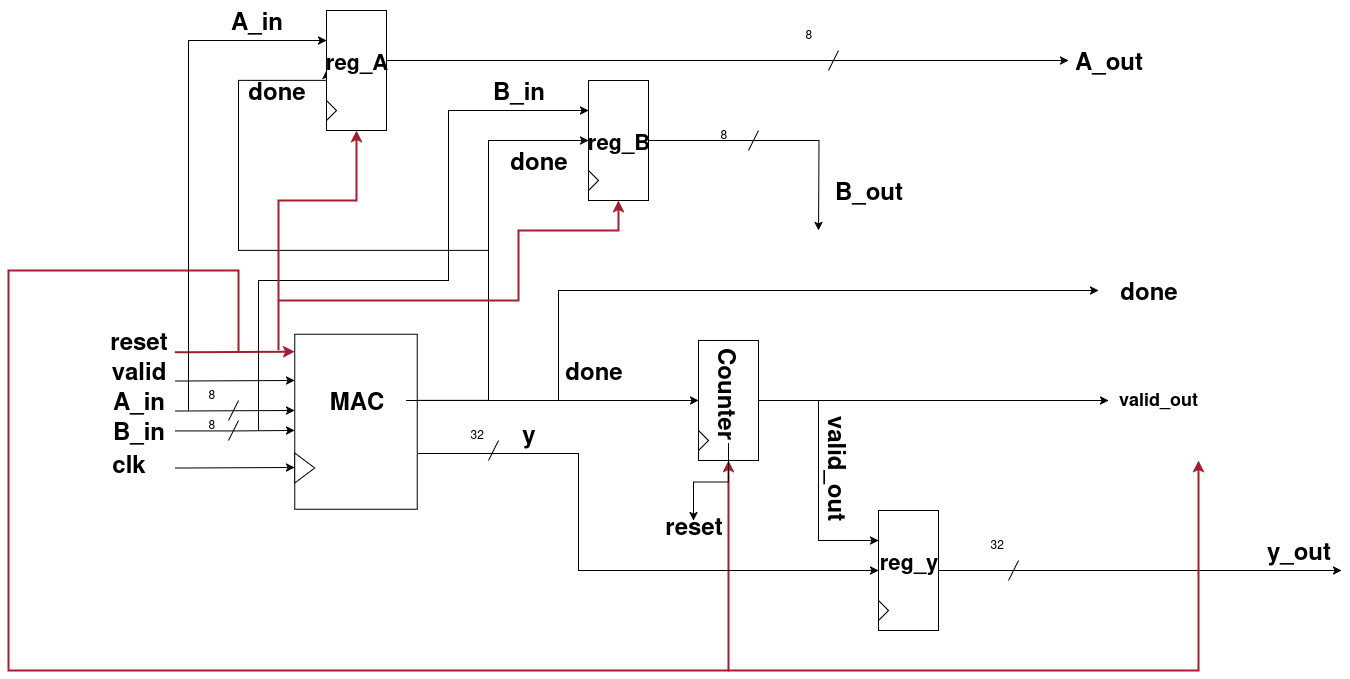
Explanation:
- Step 1:
A_in,B_in,valid, andresetgo to the MAC unit and process the same way as explained earlier. - Step 2: From the MAC unit, we get
yanddoneas outputs. doneindicates that the MAC process has been completed.- This
donesignal is passed through a counter (design explained below). - When the counter registers 7 occurrences of
done, thevalid_outflag becomes high, showing that the PE’s computations are complete. - Step 3: The
valid_outalso connects to a register. When we get 7 outputs ofyfrom the MAC unit, it confirms that the PE’s calculations are finished, and finally,y_out(32 bits) is produced.
Why count 7 times?
- In the Systolic Array Architecture, after padding, the last row and last column expand into 7 elements:
- 4 actual elements
- 3 padded zeros
- Therefore, we must count 7
donesignals to ensure that the row/column computation has finished correctly.
Role of A_out and B_out
- Whenever the
donesignal goes high,A_inandB_inare stored inreg_Aandreg_B. - These values then propagate outward as
A_outandB_out.
Why are A_out and B_out needed?
- In the systolic array, each PE must process 7 elements per row/column.
- In a 4×4 systolic array, there are 16 Processing Elements (PEs) working in parallel.
- To enable this parallel pipelined computation, each PE forwards
A_outandB_outto its neighbors. - This design ensures faster computations by reducing the number of cycles required.
Simulations:
Counter
I. PinOut:
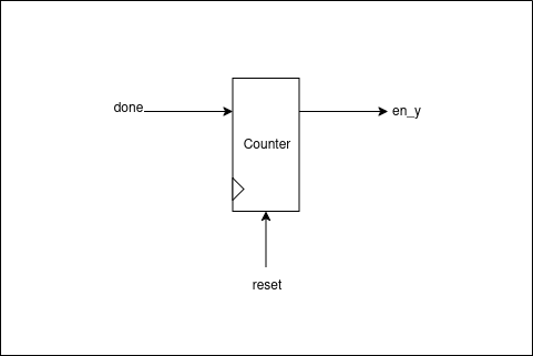
Inputs:
- reset – Resets the counter.
- done – Input pulse that needs to be counted.
Outputs:
- en_y – Goes high when the counter completes 7 counts.
II. Design Diagram
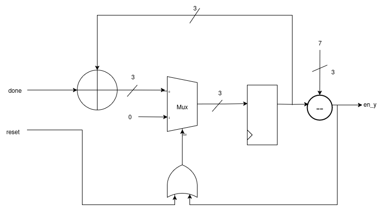
Explanation
- The input signal (
done) is added to the previous result. - The previous result is selected by a Mux.
- The selector pin of the Mux is driven by the OR of
resetanden_y. - If
resetis high oren_yis high (count complete), the Mux passes zero. - Otherwise, it passes the actual input to be stored in the register.
- A comparator checks each result.
- When the count reaches 7, the comparator output goes high, raising
en_y.
(3) Data Feeders
1. Why we used them?
We have already described the processing element. Now, since we are using a 4×4 systolic array, a total of 16 processing elements will be used.
- Each processing element takes 8-bit input.
- However, we have 7 elements in a row/column (as per the systolic array architecture).
- This makes it 7 × 8 = 56 bits.
A simple solution is to use data feeders, in which we feed 56-bit row/column data and get 8-bit elements by shifting them one by one, which are then fed to the respective registers.
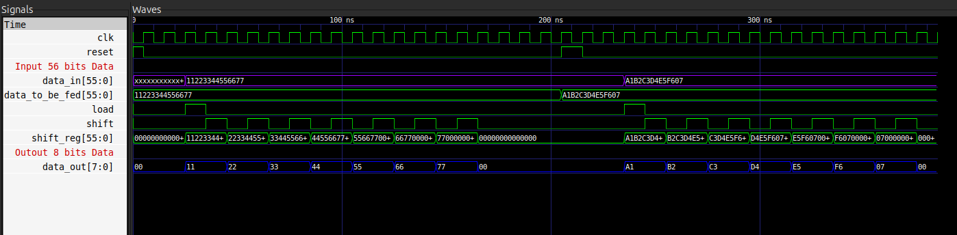
2. PinOut
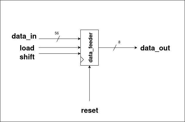
Inputs:
- data_in – 56-bit input row/column data.
- load – Load signal to initialize the feeder.
- shift – Shift signal to move data one element at a time.
- reset – Resets the internal state of the feeder.
Outputs:
- data_out – 8-bit output element, fed to the respective registers.
3. Design Diagram
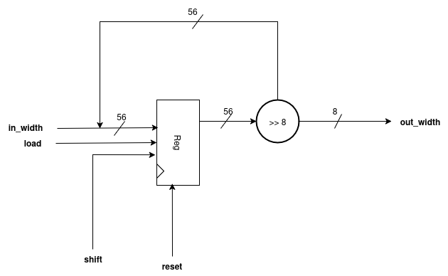
Explanation
- The
in_width(i.e.,data_in) is stored in a register wheneverloadis high andresetis off. - When the shift signal is high, the register shifts data from the Most Significant Bit (MSB).
- This process produces seven 8-bit chunks, which are then fed to the Processing Elements as individual elements of a row/column.
- These seven 8-bit chunks form the out_width, which corresponds to
data_out.
Simulations:
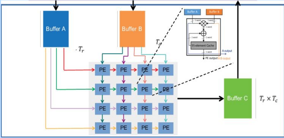
(4) Systolic Top
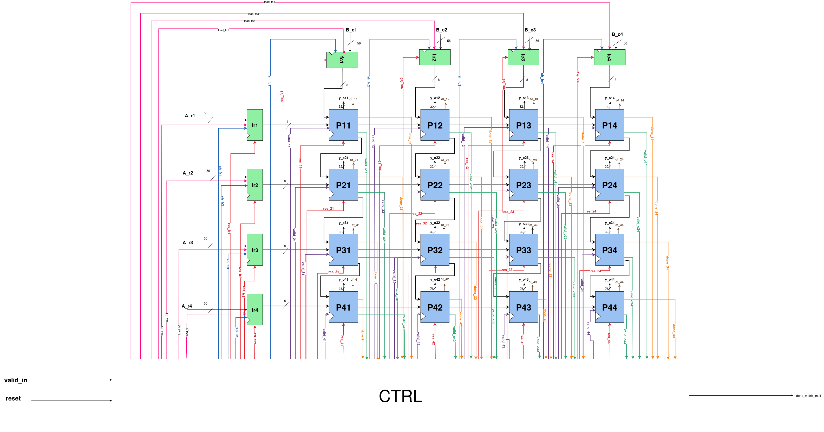
- This is how our Systolic Array Top looks after connecting all the Processing Elements and Data Feeders.
- To use this array, a proper interface is required, which is explained in the following sections.
(5) Interface
1. Interface Design Diagram
Main Parts of Interface:
1. Ready-Valid Protocol
2. Input Manager
3. Output Manager
EXPLANATION
1. READY-VALID PROTOCOL
PinOut
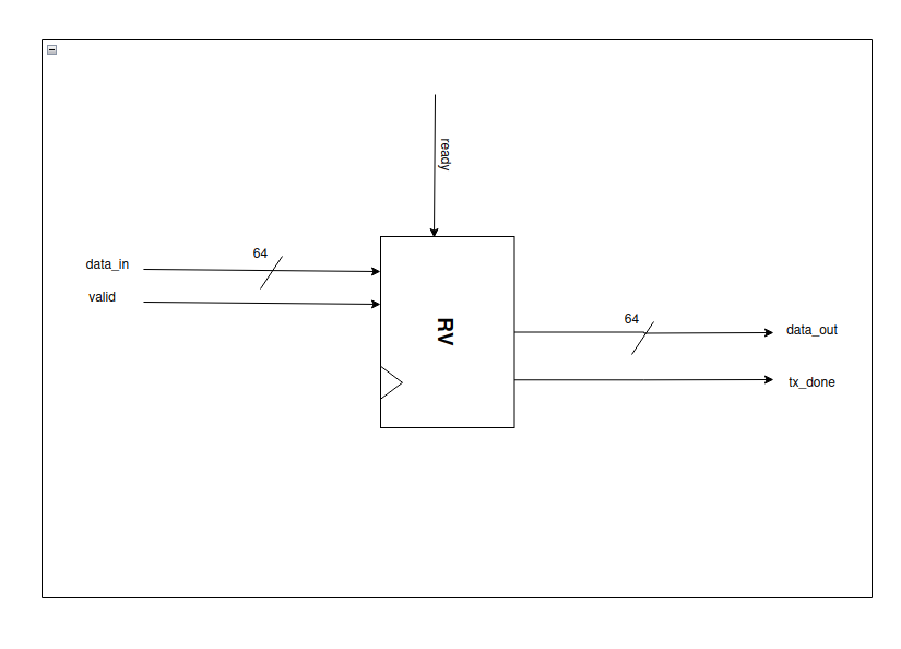
Inputs:
- ready – Indicates that the receiver is ready to accept data.
- valid – Indicates that the sender has valid data.
- data_in – 64-bit input data.
Outputs:
- data_out – 64-bit output data.
- tx_done – Goes high whenever data_out is successfully transmitted.
Design Diagram
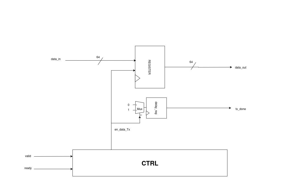
Explanation
- Whenever valid becomes high,
data_inis received. - When both valid and ready are high:
en_data_Txgoes high → handshaking occurs.data_outis produced in the next cycle (64 bits).tx_donesignal goes high whenever the respectivedata_outis available.
How does tx_done work?
en_data_Txgoes high when handshaking occurs.- A multiplexer (MUX) uses
en_data_Txas the select signal. - When
en_data_Tx = 1, the MUX outputs 1. - This output passes through a delay register, producing
tx_donein the next clock cycle.
Why use a delay register?
- Without the delay register,
tx_donewould assert one cycle earlier than the availability ofdata_out. - The delay register ensures
tx_donealigns with the exact cycle whendata_outis valid, confirming the output data is ready.
State Transition Graph (STG)
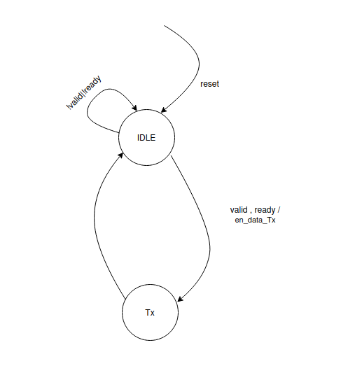
Explanation
I. IDLE
- On reset, the system enters the IDLE state.
- If either
validorreadyis low, the system remains in IDLE. - When both
validandreadyare high, handshaking occurs, and the system transitions to the Tx state.
II. Tx
- In this state,
validandreadybeing high indicate that handshaking has occurred. - The
en_data_Txsignal is asserted (goes high), initiating the data transfer. - Immediately after this, the system returns to the IDLE state.
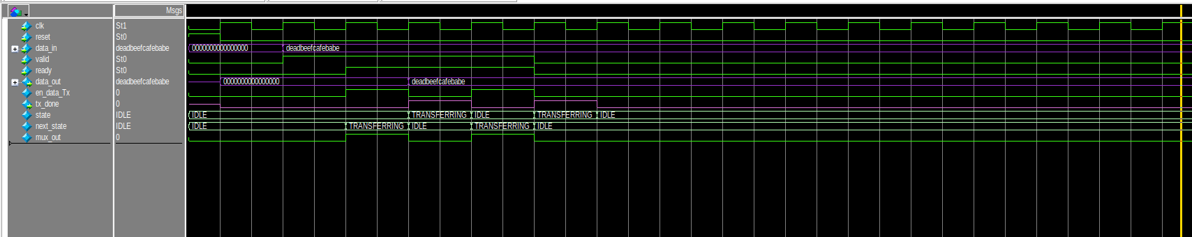
Simulations:
2. INPUT MANAGER
PinOut
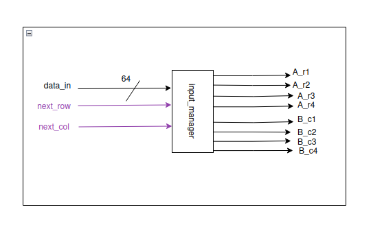
Inputs:
- data_in – 64-bit input data.
- next_row – Signal to indicate the next row of the matrix.
- next_col – Signal to indicate the next column of the matrix.
Outputs:
- A_r1, A_r2, A_r3, A_r4 – 56-bit outputs for rows 1 to 4.
- B_c1, B_c2, B_c3, B_c4 – 56-bit outputs for columns 1 to 4.
- Each row/column has 7 elements, and each element is 8 bits → 7 × 8 = 56 bits.
Working:
- The Input Manager is combined with the input datapath, which is explained in the following section.
3. OUTPUT MANAGER
PinOut
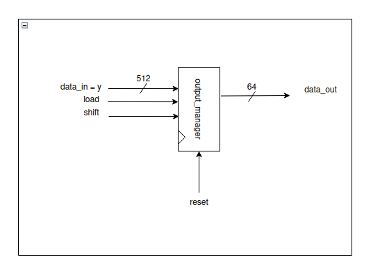
Inputs:
- load – Signal to load the input data.
- shift – Signal to shift the data.
- reset – Resets the internal state of the output manager.
- data_in – 512-bit input data (y from processing elements).
Outputs:
- data_out – 64-bit output data, produced eight times from the 512-bit input.
Design Diagram
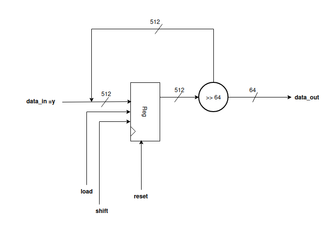
Explanation
- The Systolic Array produces 512 bits output (16 PEs × 32 bits each).
- These 512 bits serve as
data_in/yfor the Output Manager. - The Output Manager acts like a data feeder, mainly implemented as a shift register.
- The first 64 bits are taken from the MSB side when
loadis high. - For the remaining seven 64-bit chunks:
- Wait for the
shiftsignal. - Each time
shiftgoes high, the next 64-bit chunk is produced asdata_out. - In this way, the eight 64-bit outputs are obtained sequentially.
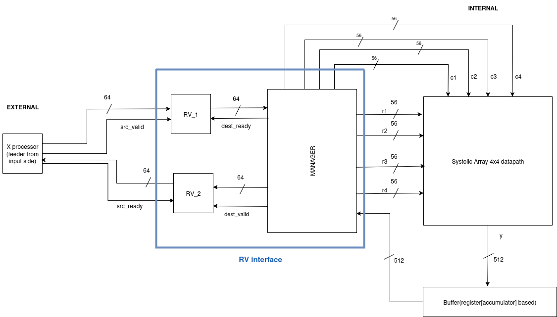
(6) Systolic Array
Main Parts of the Systolic Array
Our final Systolic Array consists of three main parts:
- Input Datapath
- Systolic Top
- Output Datapath
EXPLANATION
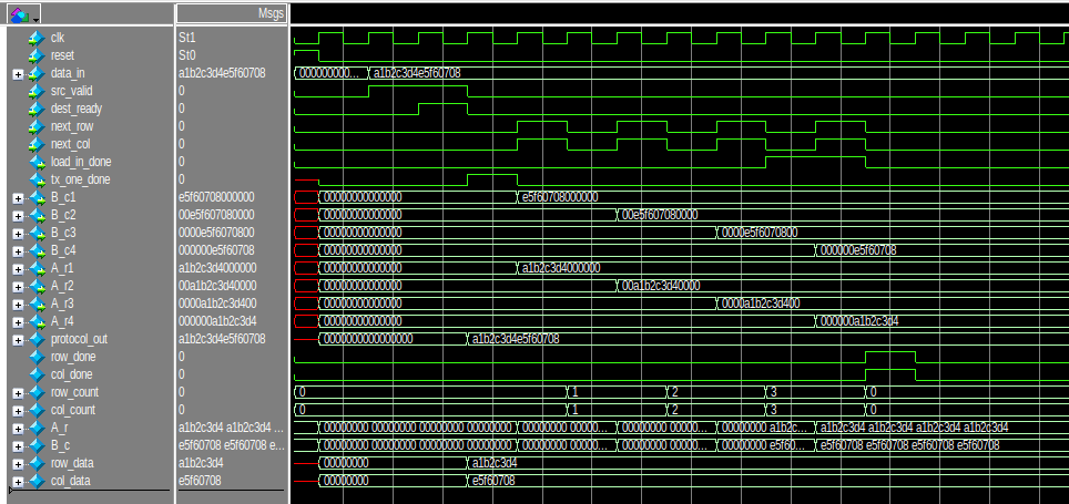
1. Input DataPath
Explanation
- The user provides a 64-bit input, which first enters the Ready–Valid Protocol (RV_1).
- When both
src_validanddest_readyare high, handshaking occurs, producing: protocol_out→ the same 64-bit input-
tx1_done→ generated in the next cycle -
The 64-bit
protocol_outis passed to the Output Manager, where it is split into two 32-bit parts: [63:32]→ row data-
[31:0]→ column data -
Row_count and col_count act as enables for registers
reg_riandreg_cj(i,j = 0 to 3) -
First row/column:
-
row_count = col_count = 0→ stored inreg_r1andreg_c1 -
Subsequent rows/columns:
- When
next_rowandnext_colgo high,row_countandcol_countincrement. -
Values are stored in
reg_r2/reg_c2,reg_r3/reg_c3, andreg_r4/reg_c4. -
When
row_countandcol_count = 3, all four rows and columns are captured. -
load_in_donesignal is asserted → indicates all inputs have been successfully loaded -
Registers holding the values:
- Rows:
reg_r1,reg_r2,reg_r3,reg_r4 -
Columns:
reg_c1,reg_c2,reg_c3,reg_c4 -
56-bit outputs generated from registers:
- Rows:
A_r1,A_r2,A_r3,A_r4 -
Columns:
B_c1,B_c2,B_c3,B_c4 -
These values are finally fed into the data feeders of the Systolic Array.
Simulations
2. Systolic Top
Explanation
- The four rows and four columns are fed into the data feeders, which pass them to the Processing Elements (PEs) as described earlier.
- Each PE produces a 32-bit output (
y_out). - Using a 4×4 systolic array, there are 16 PEs, resulting in a combined output of:
16 × 32 = 512 bits- This output is referred to as
y. - The 512-bit
yis then passed to the Output Datapath, where it is organized into eight 64-bit chunks, forming the final output. (Because64 × 8 = 512)
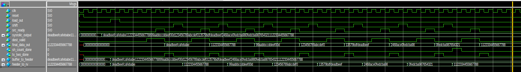
3. Output DataPath
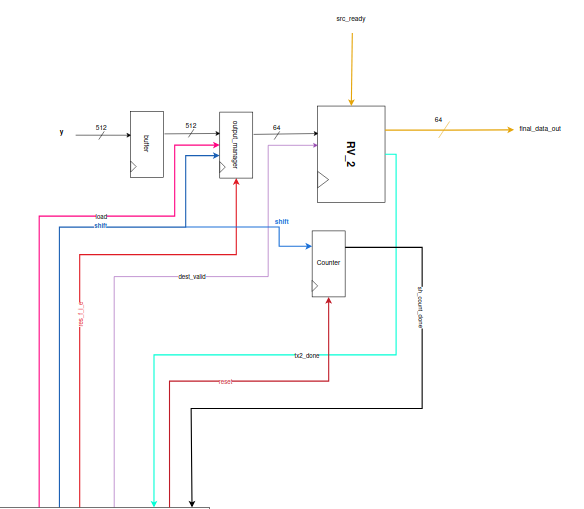
Explanation
- The 512-bit
yfrom the Systolic Top is first stored in a buffer (simple register), which outputs the stored value in the next cycle. -
This 512-bit data is then sent to the Output Manager, where it waits for the load signal.
-
When load is asserted:
- The first 64 bits (from the MSB side) are sent to the Ready–Valid Protocol (RV_2).
-
When both
dest_validandsrc_readyare high in RV_2, handshaking occurs:final_data_out→ first 64-bit output chunktx2_done→ asserted to indicate successful transfer
-
After the first
final_data_out: - The shift signal from the Output Manager is asserted.
- The next 64-bit chunk is shifted out and sent to RV_2.
-
Handshaking occurs again → second 64-bit
final_data_outwithtx2_done. -
This process continues:
- A total of 7 shifts occur → 8 final outputs of 64 bits each.
-
Since
8 × 64 = 512, the entire Systolic Array output is successfully transferred. -
The 7 shift events are monitored by a Counter:
- Counts up to 7 shifts.
- Once all shifts are completed,
sh_count_doneis asserted → indicates entire computation and output transfer complete.
Simulations
COUNTER
PinOut
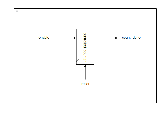
Inputs:
- enable – Starts the counting process.
- reset – Resets the counter to its initial state.
Outputs:
- count_done – Goes high when counting is complete.
Design Diagram
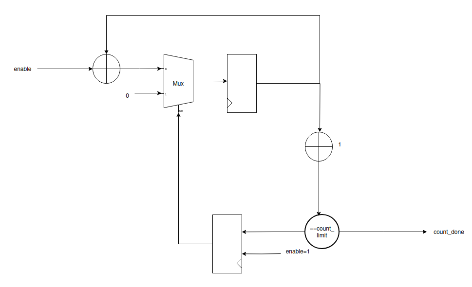
Explanation
Reset Phase
- When
rst = 1: - The counter (
count) is cleared to 0. count_donesignal is also cleared to 0.
Normal Operation (when rst = 0)
- On every posedge of clk, the counter checks the
enablesignal: - If
enable = 0→ counter holds its current value (no change). - If
enable = 1:- The counter increments by 1.
- While
count < count_limit - 1: - Only
countupdates count_doneremains 0- When
count = count_limit: count_doneasserts (1) for one clock cycle- The counter immediately resets back to 0
Key Behavior
- Counts clock cycles when enabled.
- After completing
count_limitcycles, it raises a 1-cycle done pulse (count_done). - The process repeats as long as
enableremains asserted.
FINAL SYSTOLIC ARRAY
Design Diagram
We have connected all three main parts to get the overall final Systolic Array as shown below:
State Transition Graph (STG) of Controller
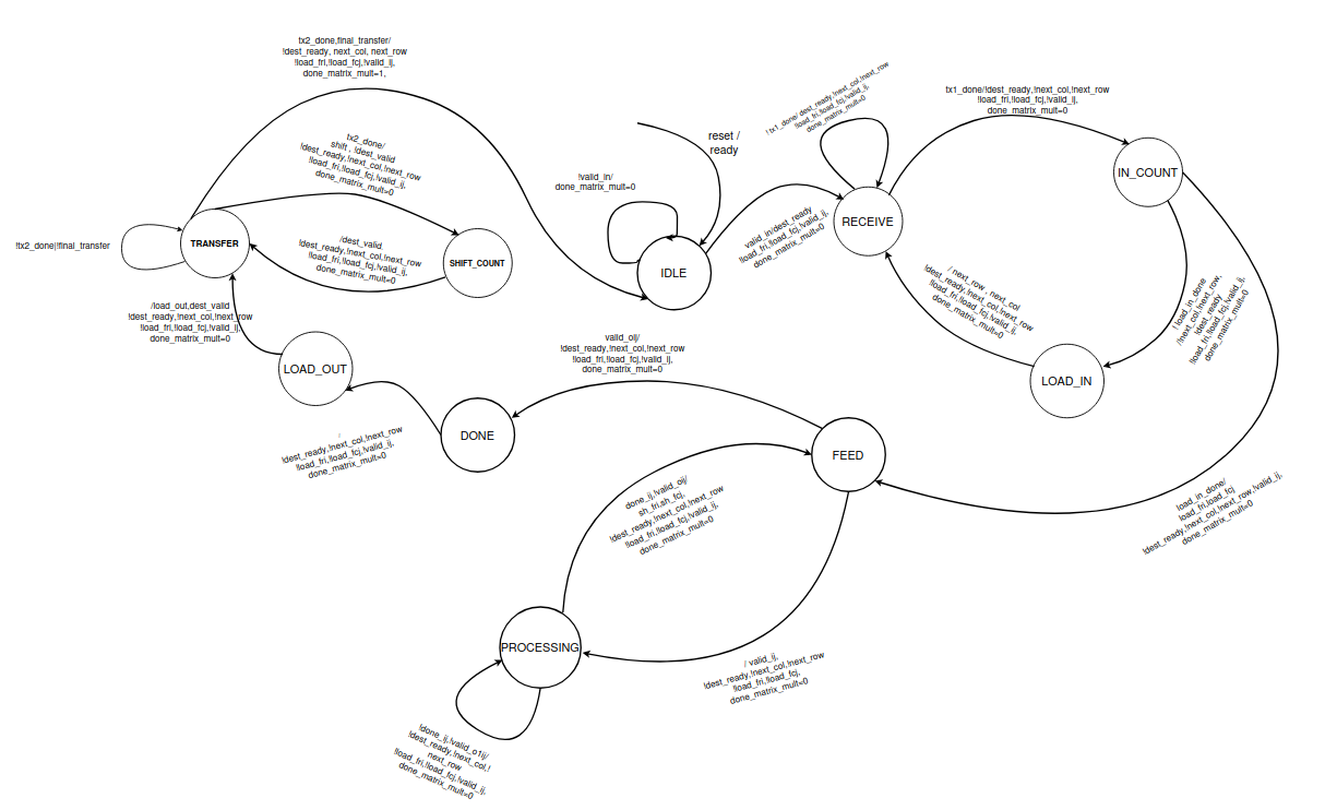
Explanation of States
I.IDLE:
- In this state, the processor is waiting for the valid_in signal.
- done_matrix_mult is 0 in this state.
II.RECEIVE:
- We reach this state when we get valid_in in the IDLE state.
- The dest_ready is set and we are waiting for a ready/valid handshake to occur.
- The handshake will occur when we receive the src_valid. It will be indicated by the tx1_done signal.
- When we receive the tx1_done signal, we will transition to the IN_COUNT state, else we will stay in RECEIVE state.
III.IN_COUNT:
- In this state, the dest_ready is set to 0.
- This state is meant to count the number of tx1_done signals after the first transition.
- It allows the data to be arranged for loading into the appropriate registers.
IV.LOAD_IN:
- While the load_in_done sigal is not set, we will move into this state. Meaning that control only moves into this state if the loading operation is incomplete.
- In this state, we wait for a cycle so that values get loaded into the appropriate registers.
- Then we unconditionally move back to the RECEIVE state for further data.
- During this transition to the RECEIVE state, it will set next_row and next_col to 1.
V.FEED:
- When the load_in_done signal is high in the IN_COUNT state, we transition into this state.
- In this state, all the load signals of the data feeders are set to 1, and hence it loads in the values and gives out 8-bits (MSBs) of data.
- After feeding, it unconditionally moves into the processing state, given that valid_o flag is not set.
- If the valid_o flag is set, we move to the DONE state.
VI.PROCESSING:
- In this state we wait till the done signals are set.
- The done signal will indicate the completion of a partial product.
- After receiving done signal, we move back to the FEED state.
- While moving into the FEED state, we set the shift signals of the feeders to 1 for a cycle, so that new elements are available to be fed into the chip.
VII.DONE:
- This state indicates the exit of the control from the systolic array and transitions into the LOAD_OUT state unconditionally.
- While doing so, it causes the buffer to be store the value of the computed product.
VIII.LOAD_OUT:
- This state transitions into the TRANSFER state unconditionally.
- While this transition, it will set the load of the final feeder to 1 and also set the dest_valid.
IX.TRANSFER:
- In this state we are waiting for the ready/valid handshake to occur.
- The handshake only happens when the src_ready signal is received.
- When it will occur, we will get the tx2_done signal. And we will transition into the SHIFT_COUNT state. During that transition, shift of the datafeeder will be set to 1 for a cycle. The dest_valid is set to 0.
- Until we get the tx2_done signal, the control will stay in this state.
- When we get tx2_done signal and also the final_transfer signal, the control jumps back to idle, setting matrix_mult_done to 1 for a cycle, indicating that the final element has been transferred.
- It also sets next_row and next_col to 1 in order to reset by overflowing their respective counters.
X.SHIFT_COUNT:
- This state transitions back into the TRANSFER state unconditionally.
- The dest_valid is set to 1 during transition.
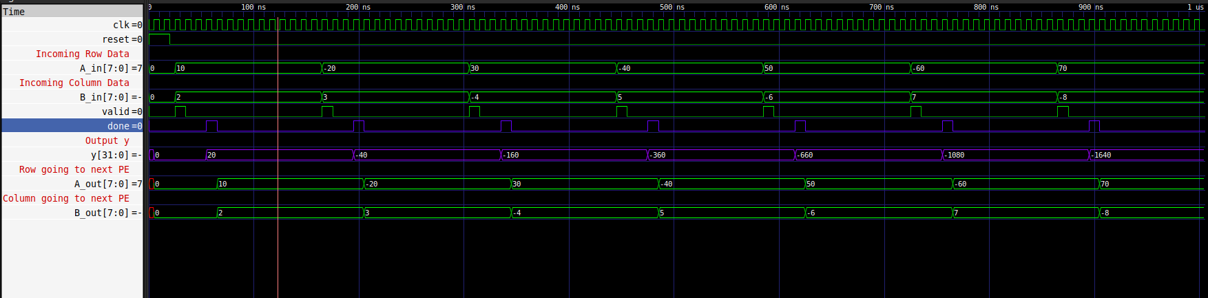
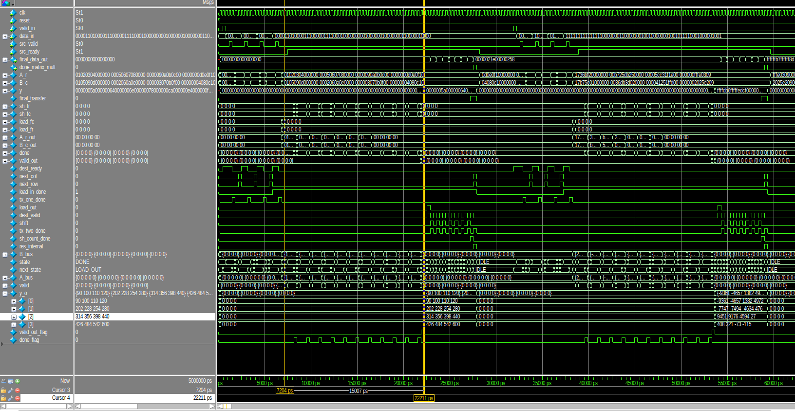
(7) TESTING
We tested by six examples , two are shown below :
Simulation:
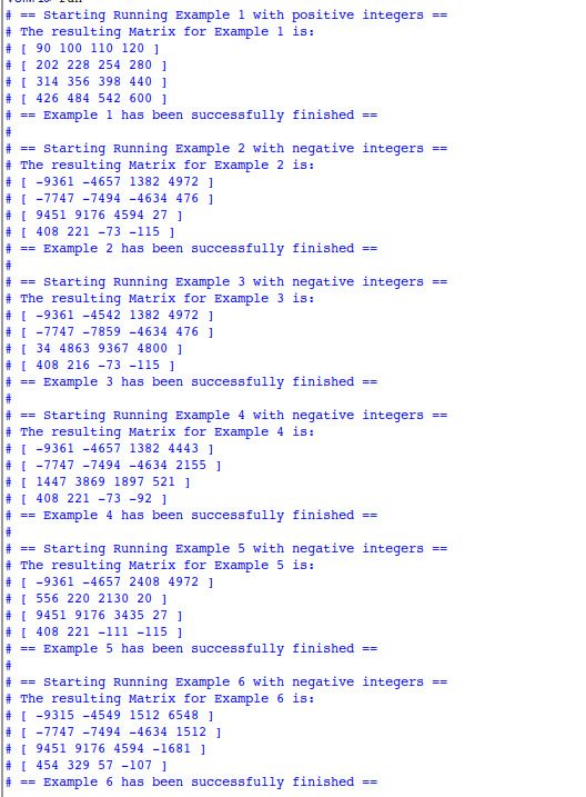
(8) RESULT
Transcript:
Benchmarks
We used a custom benchmark written in C language, which multiplied two randomly generated 8 bit 4x4 matrices into 4x4 32 bit result. We ran it on different processors 6 times and took the average of the findings. The results are shown in the table below.
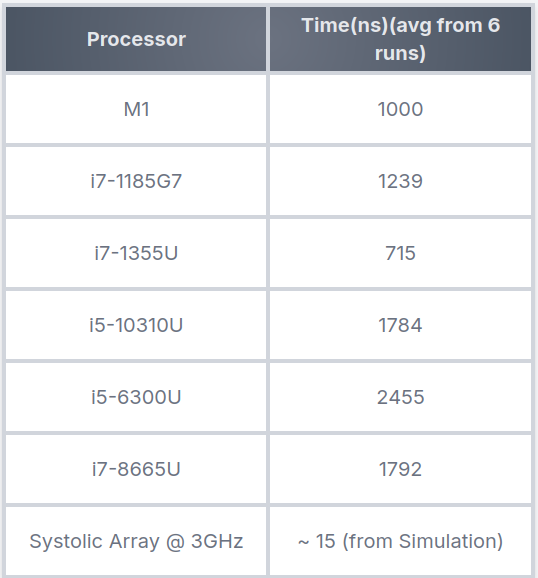
Hence we observe that the systolic array is approximately 50-160 times faster than main-stream general purpose cpus.